
Manufacturing process of solar panel
Tags:
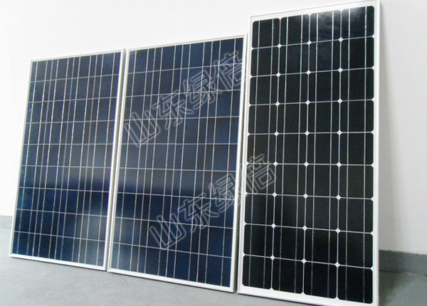
solar panel
Manufacturing process of solar panel
10 steps: slicing, cleaning, preparation of suede, peripheral etching, removal of back PN + junction, fabrication of upper and lower electrodes, fabrication of antireflection film, sintering, testing and grading
Specific manufacturing process description of solar panel
(1) Slicing: the silicon rod is cut into square silicon wafer by multi wire cutting.
(2) Cleaning: use the conventional silicon wafer cleaning method, and then use acid (or alkali) solution to remove the cut damage layer on the silicon wafer surface by 30-50um.
(3) Preparation of suede: anisotropic etching of silicon wafer with alkali solution to prepare suede on the surface of silicon wafer.
(4) Phosphorus diffusion: the coating source (or liquid source or solid phosphorus nitride sheet source) is used for diffusion to make PN + junction, and the junction depth is generally 0.3-0.5um.
(5) Peripheral etching: the diffusion layer formed on the peripheral surface of the silicon wafer during diffusion will short circuit the upper and lower electrodes of the battery. The peripheral diffusion layer shall be removed by masking wet etching or plasma dry etching.
(6) Remove the back PN + junction. The back PN + junction is usually removed by wet etching or grinding.solar panel.
(7) Making upper and lower electrodes: vacuum evaporation, electroless nickel plating or aluminum paste printing and sintering. First make the lower electrode, and then make the upper electrode. Aluminum paste printing is a widely used process.
(8) Fabrication of antireflection film: in order to reduce the input reflection loss, a layer of antireflection film shall be covered on the surface of silicon wafer. Materials for making antireflection films include MgF2, SiO2, Al2O3, SiO, Si3N4, TiO2, Ta2O5, etc. The process methods can be vacuum coating method, ion coating method, sputtering method, printing method, PECVD method or spraying method.